Currently, there are just two types of antenna analyzers: the bad ones and the expensive ones. The first type is usually built around diode detectors and has a tuning knob to set the frequency of its LC oscillator, while the second type is using expensive electronic components such as DDS and RF detector chips.
A short review of antenna and network analyzers is an article which tells the reader about outstanding achievements of the antenna analyzer building industry. It also groups many commercially and home made devices by principle of operation.
The analyzer described in this article features the following:
- Much better precision compared to analyzers based on diode detectors;
- Digitally controlled frequency with very fine steps;
- Works from several hundred kHz up to 50 MHz;
- Calibration is not needed;
- Ability to display measurement results on the built-in LCD or on the computer screen;
- Very cheap electronic components are used.
The structure diagram of the analyzer is located below:
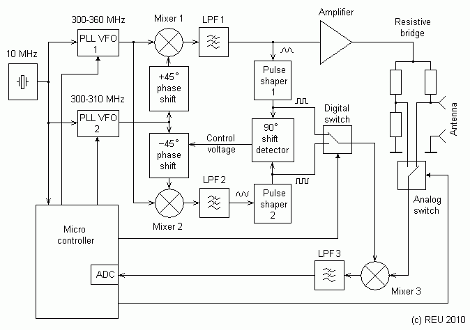
1. PLL VFOs
The PLL VFOs used in this device work at very high frequencies of about 300 MHz. The frequency at the output of the analyzer is a difference of the two PLL VFO frequencies:
f = F(PLL VFO 1) – F(PLL VFO 2)
Imagine the phase detector frequency is set to 25 kHz (which is realistic for the chosen VFO frequencies) for both PLL VFOs. The working frequency is then will change in 25 kHz steps, which are too large for measurements on lower bands (especially when the user wants to see the SWR graph of, say, 100 points over the 100 kHz range).
Instead, a “Vernier” principle is used. If phase detector frequencies are slightly different (for instance, by adding 1 to the value of the R divider of the PLL chip), much smaller steps of the difference frequency may be achieved. With the first PDF frequency of 25 kHz (R=400) and the second PFD frequency of about 24.9376 kHz (R=401), the step size drops to about 62 Hz. This is very good even for measurements on the 137 kHz band.
As a drawback of this method, we need to add 10 MHz to the tuning range of both VFOs.
2. Phase shifters
It is quite easy to built phase shifters which would be able to produce a 90-degree phase shift in the range of 300 to 310 MHz. The shifters are electrically controlled so the rest of the circuit can take care (see below) of the precise 90-degree shift.
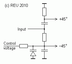
Values of the elements in phase shifting networks are calculated by using simple formulas. A varicap is a key element here, giving the ability to have the exact 90 degrees between two outputs of this circuit.
The idea of the voltage controlled phase shifters is also described in the WIPO patent WO 92/11704, “APPARATUS AND METHOD FOR GENERATING QUADRATURE SIGNALS”.
3. Mixers and low pass filters
SA612 chips are good for mixers 1 and 2. The +45° and -45° signals are fed to the VFO inputs of these chips so the result of conversion is not really sensitive to variations of their amplitude. Very simple LC-filters may be used here, since the sum of the VFO frequencies is far away from the band we are interested in.
4. Pulse shapers
To let the rest of the circuit work well, we need to make a really good, 50% duty cycle meander out of (probably distorted) sine wave. The 4.5ns Dual-Comparator-Based Crystal Oscillator has 50% Duty Cycle and Complementary Outputs article has an idea of how to do this with a small number of components. This article (in Russian language, but pictures are still international) contains a diagram of the working circuit.
5. The 90-degree shift detector
The task is very simple:
1) Take two digital signals with same frequency and a 50% duty cycle;
2) Form an analog signal which represents phase difference of these input signals;
3) Feed this signal to the phase shifter so the loop locks and the exact 90-degree shift remains regardless of the frequency of the input signals.
A trigger-based phase detector works best in this case. One can find the working implementation in the VFO of the Ten-Tec Orion radio (the full schematic diagram can be easily downloaded from the tentec.com website), although similar circuit is integrated into most of PLL chips.
6. The output amplifier and the resistive bridge
To see anything useful on the display of this analyzer, a sinewave should be fed into the antenna. This signal is taken from the output of one of the LPFs and amplified to improve the RF immunity of the device. Not a word about the resistive bridge.
7. Mixer 3 and LPF 3
Again, the SA612 is best for mixing the sinewave signal from the bridge with the square wave signal (the latter is fed into the VCO input of the mixer). Since both signals have the same frequency, only DC is left at the output of the mixer. The simple low pass filter gets rid of all harmonics.
8. The role of the microcontroller
Finally, the algorithm is as follows:
1) Calculate divider coefficients and program two PLL chips to get the frequency of interest at the antenna connector;
2) Measure the DC voltage at the output of the LPF 3 in four different positions of digital and analog switches;
3) Take these four numbers and apply a few formulas to get R,X and other parameters of the antenna;
4) Display the result on the LCD or pass it to the PC.
If you still do not understand why this analyzer needs two 90°-shifted signals, please read an article referred at the top of this page (hint: search for the “direct conversion receiver” phrase).
Denis Nechitailov, UU9JDR
19-Feb-2010